
Epitaxial Materials
Describe the layer and the substrate as one research material system.
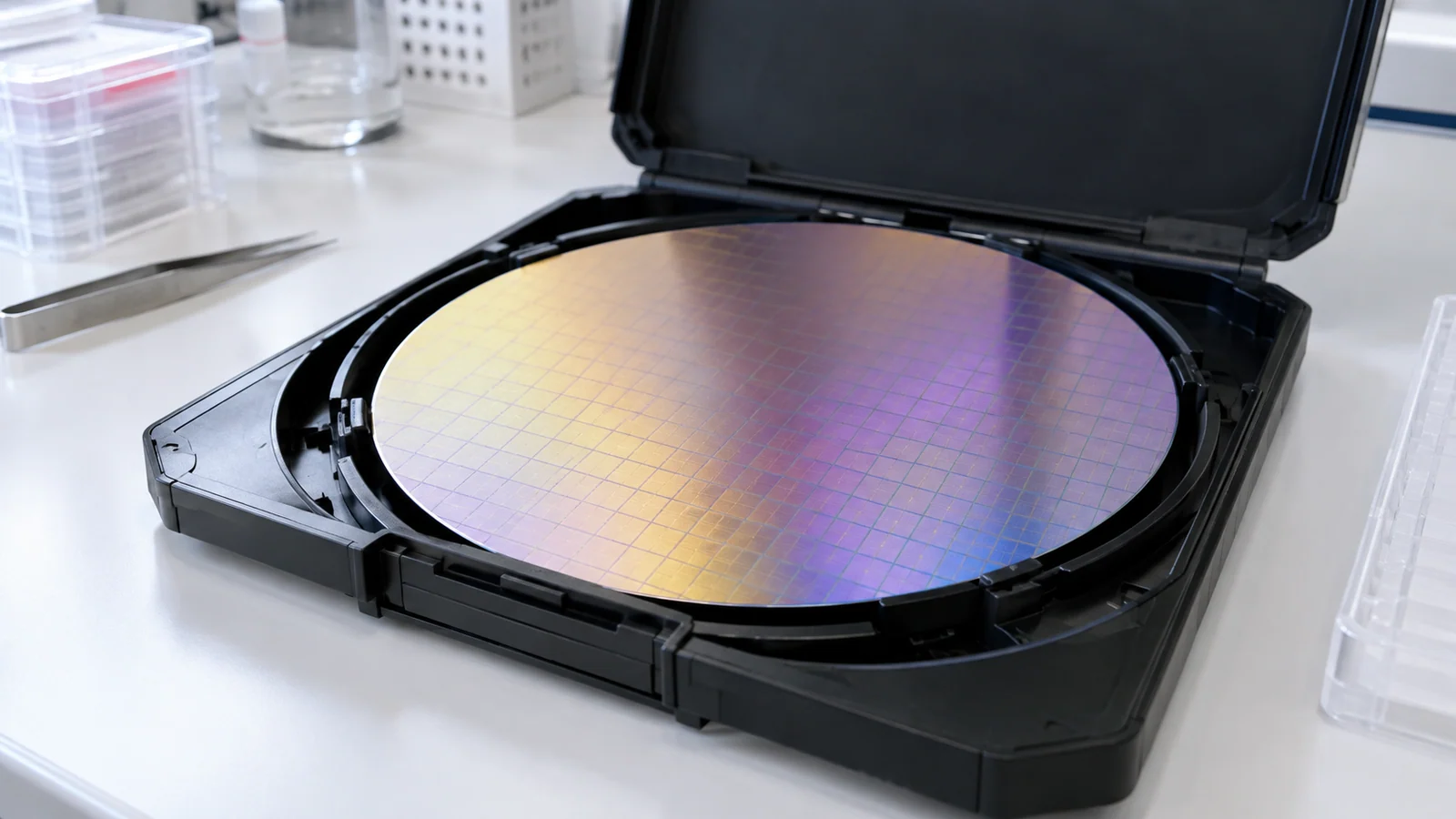
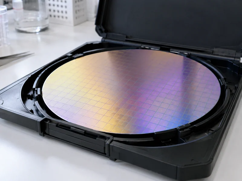
An epitaxial material specification must describe more than the name of the deposited compound. The substrate, layer structure, thickness, doping and surface condition together define what is being requested. A bare wafer and an epitaxial wafer may share a material name while serving different purposes in a research programme.
SC Science's existing materials scope includes Ga₂O₃ epitaxial wafers. Start the discussion with the intended experiment and a description of the required layer on its supporting substrate. Include crystal orientation, the target thickness and the electrical parameters that matter to your work. If multiple layers or a particular doping profile are required, provide a layer sequence or a drawing rather than relying on a general product name. Requests beyond the established material family are reviewed individually.
The enquiry should also identify which characterisation records are needed to assess the supplied material. Confirm the measurement method and reporting basis for any requested property, and distinguish target values from acceptance limits. Material availability, achievable structures and accompanying records depend on the proposed supply route. This page supports a structured materials enquiry; it does not claim in-house epitaxial growth, guaranteed device behaviour or an unrestricted range of custom layer structures.
Define the right configuration

Characterisation Records
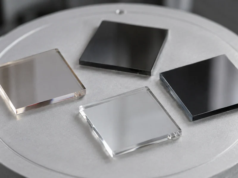
Request the records needed for incoming review. Available measurements and acceptance criteria must be confirmed for the proposed material.
Typical Applications
- ·Gallium oxide device research
- ·Epitaxial layer characterisation
- ·Process and contact development
- ·Comparative studies of specified layer structures
What to Include
- ·Substrate and epitaxial layer identity
- ·Layer sequence, thickness and orientation
- ·Doping or electrical property requirements
- ·Requested measurements and acceptance limits
Tell us what your application needs
Share the operating conditions, interfaces and constraints that matter to your work.